The 15th European Microscopy Congress
Manchester Central, United Kingdom
16th - 21st September 2012
New FE-SEM & AFM techniques offer unprecedented glimpse into graphene
Agilent Technologies has recently introduced novel field-emission scanning electron
microscopy (8500 FE-SEM) and atomic force microscopy (AFM) methods for studying the
properties of graphene at the nanoscale. As a new member of the carbon family, graphene,
a single layer of pure carbon atoms with a hexagonal arrangement, has stimulated
extensive interest due to its remarkable physical properties. Current research activities
on graphene primarily comprise property simulations, controlled synthesis, characterizations,
and exploration of potential applications.
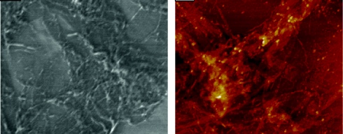
For many applications, imaging the morphology of graphene by using a scanning electron
microscope is needed; this approach is quite challenging, however. To reveal the
surface details of such a thin layer with nanoscale features, imaging at low beam
voltages is beneficial, especially for graphene on nonconducting substrates. Low-voltage
FE-SEM (<5 kV) provides a straightforward technique for imaging energy-sensitive
materials with high resolution. For nonconducting samples, coating might be eliminated
due to the possible charge equilibrium achieved on the specimen’s surface.
Low-voltage FE-SEM imaging of graphene on different substrates has now been demonstrated
in which secondary electron imaging, backscattered electron imaging, and topographic
imaging modes have been used to study the surface morphologies of graphene samples
at a broad range of magnifications. Tuning the beam voltage (down to 500 V) has been
tested as an effective method to control the charging problem caused by insulating
substrates beneath the graphene layer. This imaging technique can be used in graphene-related
research such as quality check, impurity identification of engineered graphene materials,
and device fabrication.
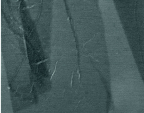
In addition to the low-voltage FE-SEM imaging discussed above, Agilent uses a frequency-modulated
Kelvin force microscopy (FM-KFM) technique that enhances the utility of AFM for graphene
studies. Researchers using atomic force microscopy are often compelled to utilize
optical methods to identify graphene due to its unique optical properties. In order
to identify graphene using AFM, counting the thickness offers the most reliable method.
Unfortunately, this approach has shortcomings when graphene layers are grown on an
opaque substrate or a substrate with uneven flatness.
Alternatively, the use of a new “frequency modulation electrostatic force” technique
reveals the electrical potential variation generated by the contact interface between
the graphene and substrate, while the dC/dZ signal can clearly differentiate between
the graphene and substrate. Combining signal contrast from multiple channels, this
FM-KFM method allows researchers to study and identify graphene without using optical
techniques.