ASTAR: Nanoscale EBSD-like technique in TEM case study: nanowires reveal their secrets
Spatial resolution of orientation imaging via conventional electron backscattered
diffraction (EBSD) analysis in SEM-FEG microscopes is limited to 50 nm. The use
of the recently developed transmission electron microscope (TEM) based technique
coupled with electron beam precession, known as ASTAR, offers the possibility to
acquire reliable orientation/phase maps with a spatial resolution down to 1 nm for
FEG TEM. The technique, which can be used with nearly all TEM, consists of scanning
the electron beam, in nanoprobe mode, over the specimen area while Precession Electron
Diffraction (PED) spot patterns are collected and indexed automatically through template
matching. ASTAR can be used in the investigation of the micro-structure / micro-texture
of nanocrystalline materials (metals, ceramics, minerals, thin films, semiconductors
and nanoparticles). Here we present a case study of nanowire texture revealed with
ASTAR in a 120 kV TEM microscope.
III-V semiconductor nanowires represent the forefront of solid state physics and
technology. Nanowires are quasi one-dimensional crystals that can be heterostructured
in different sectors having different chemical composition and crystal structure.
They are grown by chemical beam epitaxy (CBE) from a III-V wafer with the Au-assisted
growth method. In this method the wafer is coated with a thin layer film that transforms
into small Au nanoparticles during a dewetting thermal treatment in the CBE chamber.
Au nanoparticles act as a catalyst and drive the growth of the nanowire out from
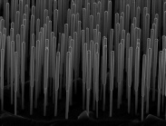
the wafer. In the final stage of the growth the wafer resembles a forest of nanowires
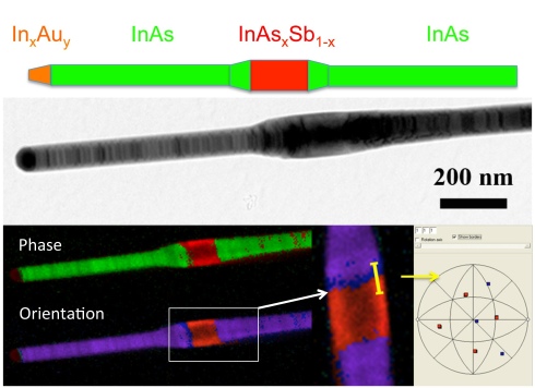
each with its own Au nanoparticle on top (fig. 1). The growth of heterostructured
nanowires is a challenge, especially if the two crystal structures, which must be
piled up on top of each other, have a large lattice mismatch. This is the case of
the InAs/InAs1-xSbx/InAs heterostructure, which can only be grown in nanowires, where
the strain can be relaxed at the free surface, but not in a two-dimensional growth.
ASTAR is able to identify where the cubic Sb sector is located between the bottom
and top hexagonal InAs stems. It can determine the relative orientation (10 nm texture
map resolution) of the two crystal structures and is able to recognize twinned layers
inside the cubic Sb sector (fig. 2). These structural details are crucial to foresee
and design the proper electrical and transport properties of the heterostructure.
Electron microscope: Zeiss Libra 120 -ASTAR
Research Group: Mauro Gemmi (Istituto Italiano di Tecnologia, Pisa, Italy), Lucia
Sorba (CNR-NANO, Pisa, Italy), Daniele Ercolani (Scuola Normale Superiore, Pisa,
Italy). Ref: Ercolani et al. Nanotechnology 23 (2012) 115606
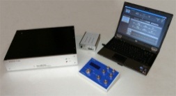
Fig.1: (left) overview of ASTAR hardware components, (right) SEM image of a forest of InAs/InAsSb
Fig. 2 (Top) Model and bright field image of a InAs/InAs1-xSbx/InAs heterostructured nanowire. (Bottom) Phase and orientation mapping of the same nanowire. In the phase map the cubic zinc blende structure of the Sb part is identified (red) while the orientation map shows that it separated from the hexagonal wurtzite InAs stem by a twinned sector of 30 nm (blue). At the bottom left a pole figure calculated trough the twin boundary is displayed